by Sebastian Tomczak. Please email stomczak@e-access.com.au for blah-blahing
Please note that the construction of a square wave oscillator using a hex inverter integrated circuit and then using it to control a digital binary counter integrated circuit is taken from the excellent reference:
pp 111-139. Collins, Nicolas 2006, Handmade Electronic Music: The Art of Hardware Hacking, TF-ROUTL.
CONTINUE AT OWN RISK!
All of the schematics presented here in the 'Sound Devices' section operate on the premise of digital logic - that is, a reliance on two individual states used to represent information.
Multiple states can be encoded as information when considering a set of 1s and 0s. Think about the number four. Four cannot be represented by a 1 or a 0 alone. However, when one considers three or more 1s and 0s in combination with each other, the number four can be encoded. For example:
0 0 0 = 0
0 0 1 = 1
0 1 0 = 2
0 1 1 = 3
1 0 0 = 4
Electricity is able to represent the idea of a 1 and a 0 quite easily. A 1 can be represented, for example, by the positive voltage rail of a direct current circuit. A 0 can be represented, for example, by the zero voltage or ground rail of a direct current circuit.
There are three types of integrated circuits used in these mini-projects. All of the chips involved operate with high (1) and low (0) signals. By combining the functions of these chips in various ways, it is possible to create various types of sequencers and related devices. They all belong to the 40XX family of chips. The good news is that they operate between 3V and 15V and use up very little power. They are common and are available at physical outlets such as Dick Smith Electronics, Jay Car, Aztronics, Altronics as well as online retailers such as Futurlec.


|
|
The 40106 is a hex inverter. It has six seperate stages. Each stage has an input and an output. When a high (1) is presented at an input of a stage, the output goes low (0). When a low (0) is presented at an input of a stage, the output goes high (1).
Function
In the context of the schematics presented on this page, the 40106 is a source of up to six oscillators. This is achieved by feeding an output of a stage back into the input.
|
|
The 4040 is a binary counter / divider. Although this may sound daunting, what it actually does is very simple. It has a single input. If a square wave is applied to this input, the outputs (labelled Q1 to Q12) each oscillate at a rate related to the input freqeuncy. The reset pin should be kept low.
Q1 oscillates at a frequency that is half of the input frequency. Q1 at one quarter. Q3 at one eighth and so on. If the output frequencies are within the human hearing range, they will sound one octave apart - with Q1 being the highest and Q12 being the lowest (eleven octaves below Q1).
This relationship can be represented as a timing diagram, shown below:
CK -_-_-_-_-_-_-_-_-_-_-_-_-_-_-_-_-_-_-_-_-_-_-_-_-_-_-_-_-_-_-_-_

Q1 --__--__--__--__--__--__--__--__--__--__--__--__--__--__--__--__

Q2 ----____----____----____----____----____----____----____----____

Q3 --------________--------________--------________--------________

Q4 ----------------________________----------------________________

Q5 --------------------------------________________________________

and so on
Function
In the context of the schematics presented on this page, the 4040 creates timed parallel digital control signals.
|
|
The 4051 is an eight channel analog multiplexer / demultiplexer. Once again, this description might seem a little mysterious. And also once again, what it actually does is quite simple. The inhibit and low input pins should be tied to ground.
The 4051 has eight channels (numbered 0 - 7) and a common connection pin. Depending on the status of the three address pins A,B and C in combination determines which of the eight channels passes its present voltage to the common connection pin. Logically, we can think of the eight channel pins as eight gates, of which only one can be open (ie. connected to the common pin) at any one time. The relationship between which gate is currently selected via the three address pins can be seen below in the truth table.
| Address Pin C | Address Pin B | Address Pin A | Selected Gate |
| high (1) | high (1) | high (1) | 7 |
| high (1) | high (1) | low (0) | 6 |
| high (1) | low (0) | high (1) | 5 |
| high (1) | low (0) | low (0) | 4 |
| low (0) | high (1) | high (1) | 3 |
| low (0) | high (1) | low (0) | 2 |
| low (0) | low (0) | high (1) | 1 |
| low (0) | low (0) | low (0) | 0 |
Function
In the context of the schematics presented on this page, the 4051 outputs different values of voltage or resistance over time (depending on the state of the address pins).
The sound making devices listed here by no means exhaust the possiblites of using one or more of the IC's. Experimentation is very much encouraged. Many variations and extensions are possible. Keep this in mind.
A number of things are required in order to build any of the devices on this page.
Please note that the construction of a square wave oscillator using a hex inverter integrated circuit and then using it to control a digital binary counter integrated circuit is taken from the excellent reference:
pp 111-139. Collins, Nicolas 2006, Handmade Electronic Music: The Art of Hardware Hacking, TF-ROUTL.
Schematic
|
Breadboard Examples
[with resistor]
[with potentiometer] |
Parts list
The 40106 looks like it only has two pins. This is because only one of the six inverter stages are shown. The triangle representing the inverter shows the signal direction - the apex line is the output whilst the line going into the base is the input. The numbers just outside of the inverter stage are the physical pin numbers of the IC legs.
The basic idea is pretty simple. When the inverter stage is low on the input, the output goes high and vice-versa. By feeding the output back into the input, the inverter is constantly chaning between between being high and low. Thus, it outputs a square wave.
The frequency of the square wave is determined by the values of the capacitor and the resistor. Begin with using a 0.1uF cap and a 10KΩ resistor. Try replacing the cap with a higher value. Replace the 10KΩ resistor with a 10KΩ pot by connected the output of the 40106 to one of the end legs and the input of the 40106 to the middle leg.
Audio Examples
[oscillator with potentiometer]
Please note that the construction of a square wave oscillator using a hex inverter integrated circuit and then using it to control a digital binary counter integrated circuit is taken from the excellent reference:
pp 111-139. Collins, Nicolas 2006, Handmade Electronic Music: The Art of Hardware Hacking, TF-ROUTL.
Schematic
|
Breaboard Example
|
Parts list
The state of the three control oscillators in combination determines which gate of the 4051 is open. A resistance ladder creates different pitches for the fourth oscillator (whose output is connected to the overall output) depending on which gate is currently active. Resistors in series have a sum resistance. When gate 7 is active, the resistance is at maximum (ie. 8 x 22KΩ). When gate 0 is active, the resistance is at mimimum (ie. 1 x 22KΩ). By changing the frequencies of the three oscillators, interesting control structures can appear in relation to which pitches are selected when.
Looking at the schematic, the 4051 IC has its pin functions printed inside and the physical pin leg numbers printed outside.
Audio Example
[arp with control osc tempo changes]
Please note that the construction of a square wave oscillator using a hex inverter integrated circuit and then using it to control a digital binary counter integrated circuit is taken from the excellent reference:
pp 111-139. Collins, Nicolas 2006, Handmade Electronic Music: The Art of Hardware Hacking, TF-ROUTL.
Schematic
|
Breadboard Example
|
Parts list
The 40106 is used to create two oscillators. The first oscillator is connected to the clock input of the 4040. The first three outputs of the 4040 are connected to the address pins of the 4051 and thus 'step through' the eight gates.
A resistance ladder creates different pitches for the second oscillator (whose output is connected to the overall output) depending on which gate is currently active. Resistors in series have a sum resistance. When gate 7 is active, the resistance is at maximum (ie. 8 x 22KΩ). When gate 0 is active, the resistance is at mimimum (ie. 1 x 22KΩ).
It is recommended to use 1% or 2% (ie. not 5%) accurate resistors for the pitch values if planning to make more than one sequencer to be played at the same time. By rearranging the relationship between the 4040 output pins and the 4051 address pins, the sequence of the pitches will change accordingly. By replacing the resistance ladder with a 8 pots, the pitches will be changeable in real time.
To understand the logic of this circuit, consider the following timing diagram of the 4040 IC.
CK -_-_-_-_-_-_-_-_

Q1 --__--__--__--__

Q2 ----____----____

Q3 --------________
The clock signal is provided by the control oscillator and is connected to the input of the 4040 IC. Q1, Q2, Q3 are the first three outputs from the 4040 IC. Now, imagine that there is a connection between the outputs from the 4040 and the address inputs of the 4051, like so:
4040 Q1 --__--__--__--__ A 4051

4040 Q2 ----____----____ B 4051

4040 Q3 --------________ C 4051

Time    1 2 3 4 5 6 7 8
The 'time' component in this diagram shows the divisions of the combination of the three square waves into individual states. The smallest increment of time is when the current state changes into a different one. This is equal to double the frequency of the wave with the highest frequency (in this case Q1).
Going back to the truth diagram of the 4051, the following logic applies:
| Address Pin C | Address Pin B | Address Pin A | Selected Gate |
| high (1) | high (1) | high (1) | 7 |
| high (1) | high (1) | low (0) | 6 |
| high (1) | low (0) | high (1) | 5 |
| high (1) | low (0) | low (0) | 4 |
| low (0) | high (1) | high (1) | 3 |
| low (0) | high (1) | low (0) | 2 |
| low (0) | low (0) | high (1) | 1 |
| low (0) | low (0) | low (0) | 0 |
Thus, it can be said that as the time value increases from one to eight, the gate that is open on the 4051 decreases from 7 to 0.
| Time | Q3 = C | Q2 = B | Q1 = A | Selected Gate |
| 1 | high (1) | high (1) | high (1) | 7 |
| 2 | high (1) | high (1) | low (0) | 6 |
| 3 | high (1) | low (0) | high (1) | 5 |
| 4 | high (1) | low (0) | low (0) | 4 |
| 5 | low (0) | high (1) | high (1) | 3 |
| 6 | low (0) | high (1) | low (0) | 2 |
| 7 | low (0) | low (0) | high (1) | 1 |
| 8 | low (0) | low (0) | low (0) | 0 |
This concept is the basis for all the time-based changes presented in the circuits found on this page. This concept can be easily extended and modified.
Audio Examples
[standard address sequencer with tempo change]
[sequencer address manipulation one]
[sequencer address manipulation two]
[sequencer address manipulation three]
Please note that the construction of a square wave oscillator using a hex inverter integrated circuit and then using it to control a digital binary counter integrated circuit is taken from the excellent reference:
pp 111-139. Collins, Nicolas 2006, Handmade Electronic Music: The Art of Hardware Hacking, TF-ROUTL.
Schematic
|
Breadboard Example
|
Parts list
The 40106 is used to create two oscillators. The first oscillator is connected to the clock input of the 4040. The first three outputs of the 4040 are connected to the address pins of the 4051 and thus 'step through' the eight gates.
A resistance ladder creates different amplitudes for the second oscillator (whose output is connected to the overall output) depending on which gate is currently active. Resistors in series have a sum resistance. Thus, a voltage divider with different resistances on one side is created which controls the amplitude of the sound oscillator. When gate 7 is active, the resistance is at maximum (ie. 8 x 22KΩ). When gate 0 is active, the resistance is at mimimum (ie. 1 x 22KΩ). R1 changes the speed of the envelope, R2 changes the pitch of the waveform and R10 changes the sensitivity of the envelope generator.
By rearranging the relationship between the 4040 output pins and the 4051 address pins, the sequence of the amplitude values can be changed and extended over time.
Audio Examples
[envelope gen sensitivity adjust]
[envelope gen address manipulation one]
[envelope gen address manipulation two]
Please note that the construction of a square wave oscillator using a hex inverter integrated circuit and then using it to control a digital binary counter integrated circuit is taken from the excellent reference:
pp 111-139. Collins, Nicolas 2006, Handmade Electronic Music: The Art of Hardware Hacking, TF-ROUTL.
Schematic
|
Parts list
This is basically a combination of the basic pitch sequencer and the envelope generator. The Q1, Q2 and Q3 outputs of the 4040 control the amplitude envelope by being connected to the address pins of the second 4051. The Q4, Q5 and Q6 outputs of the 4040 control the pitch by being connected to the address pins of the first 4051. Consider that Q1, Q2 and Q3 will complete an entire period of eight states for every single state change generated by Q4, Q5 and Q6.
By rearranging the relationship between Q1, Q2, Q3, Q4, Q5 and Q6 with the address pins of the two 4051 ICs, interesting musical structures can occur. R1 controls the overall speed of the sequencer. R17 controls the overall volume output.
Please note that the construction of a square wave oscillator using a hex inverter integrated circuit and then using it to control a digital binary counter integrated circuit is taken from the excellent reference:
pp 111-139. Collins, Nicolas 2006, Handmade Electronic Music: The Art of Hardware Hacking, TF-ROUTL.
Schematic
|
Breadboard Examples
[with dip switch]
[without dip switch] |
Parts list
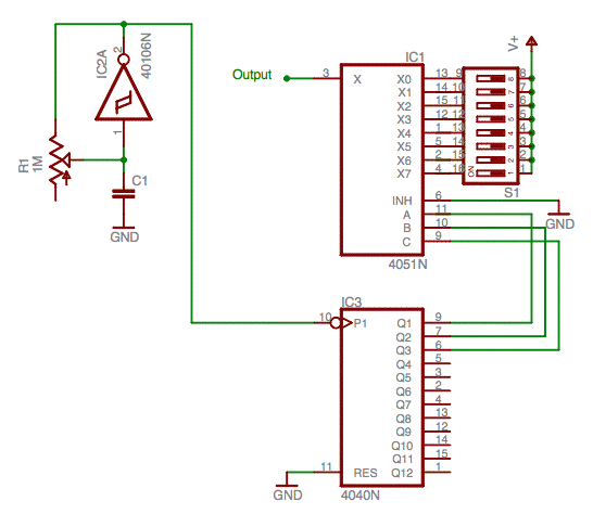
This is a lateral adaption of the basic seqeuncer. Instead of controlling the resistance that controls the frequency of an oscillator, an eight way switch allows voltage to either pass through or not over eight points in time, forming an eight stage one-bit custom waveform generator. The positions of the eight switches are a direct representation of the resulting waveform. R1 controls the frequency of the custom waveform.
This circuit can be made with or without the dip switch. If it is made with the dipswitch, the input gates on the 4051 are left floating and this effects the waveform. A true one-bit waveform can only be achieved by tying the floating lines to ground. This can be done by directly connecting the gates to either high or low to create a custome waveform. However, the dipswitch allows for an easier to use interface.
Please note that the construction of a square wave oscillator using a hex inverter integrated circuit and then using it to control a digital binary counter integrated circuit is taken from the excellent reference:
pp 111-139. Collins, Nicolas 2006, Handmade Electronic Music: The Art of Hardware Hacking, TF-ROUTL.
Schematic
|
Breadboard Example
|
Parts list
This is an extension of the 1 bit custom waveform generator. Instead of simply high / low signals being controlled, the potentiometers are used as voltage dividers and present at their middle pin a voltage between high and low.
Audio Example
[ custom waveform gen with changing waveform]